
schematics should show intent rather than reailty
When reviewing schematics I will tend to find that people have designed their schematics to directly reflect the reality of what they are building. This is not a bad thing per say, however this can and does cause information about the circuit to be lost. This in turn means when reviewing the schematic the reviewer can not tell if what you are planning to implement and can not therefor give adequate feedback. So to solve this problem the schematic that you create should show your intent of what goes there rather than what is actually there. For example a common act that causes confusion is something like this:
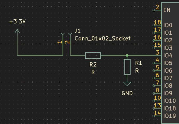
Here the user has connected a connector with a current limiting resistor to a pin of their microcontroller.
When looking at this the first thing I ask is “what is going on that connector”, most of the time it will just be a button.
And if it is just a button then I may suggest to the user to add a capacitor for debouching so they don’t have to implement it in code.
However, this could also be a switch and then that suggestion would be useless.
Furthermore, this could even be a connector to an LED that they are sinking through the microcontroller.
So as you can see that just having a single connector to say something is going to go here does not give the reviewer enough information to make an informed decision.
Therefor my suggestion is to make the schematic reflect your intention instead.
So if you are planning on using a switch then just replace the connector symbol with a switch instead as shown:
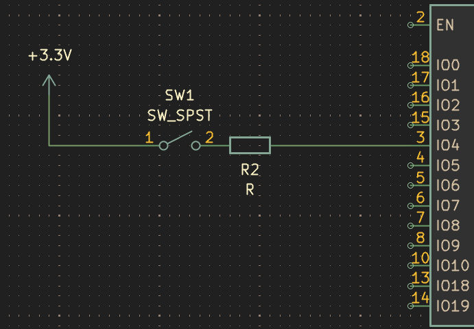
Or if its a button then use a button symbol or an led symbol if its an LED.
Then just keep the footprint the same as the connector before.
However i would add that this still isnt clear enough as this now implies that this switch is on the PCB itself.
This now contrast with the pervious symbol as it showed there was something going off board.
You could fix this by adding a note next to the switch as can be seen below or even moving the wires and adding a box around it to show it’s off the PCB.
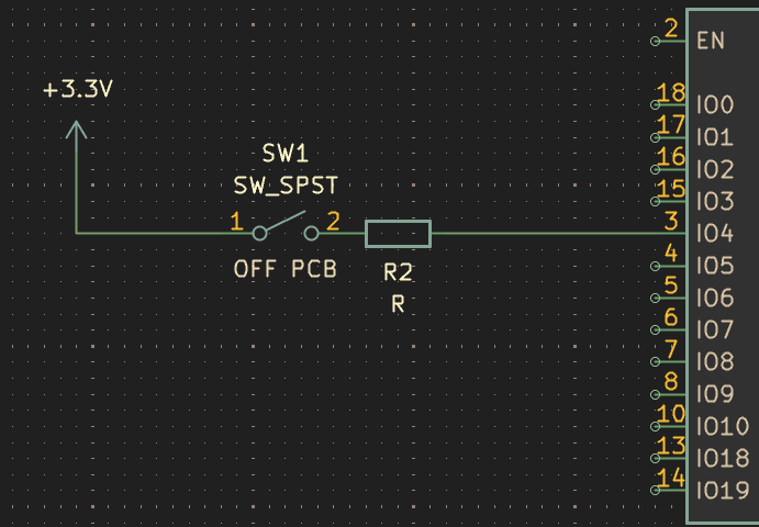
Although these fixes now reflect your intent on the PCB they don’t truly reflect the reality of your PCB.
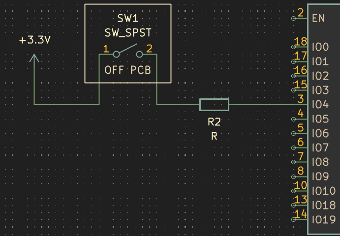
I know ive just been going on about how your schematic show should the intent of what your doing not the reality.
However, the best way to show your intent is to show the exact reality of how It’s going to be implemented.
Therefor, you can instead implement the switch like what is seen below, with both the connector on the board the connector off the board and the switch itself.
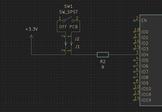 This now show both your intention behind the design and the exact reality of the design itself.
Additionally, this implemention also give the extra benefit of automatically including these items in the BOM of your PCB.
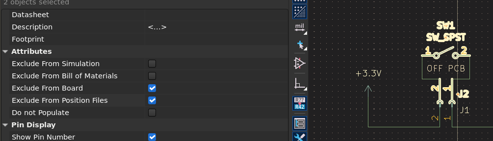
Lastly make sure to give these parts the attributes of
This now show both your intention behind the design and the exact reality of the design itself.
Additionally, this implemention also give the extra benefit of automatically including these items in the BOM of your PCB.
Lastly make sure to give these parts the attributes of exclude from board and exclude from position files.
These attributes make it, so these parts don’t need footprints as well as do not need to be routed on the PCB.
To conclude you should attempt to show the whole reality of your design rather than just the parts that sit on the PCB.